
Photonics for 5G Networks
Date: 2018-05-02Number: 1836Robero Sabella, Ericsson
IEEE 5G Tech Focus: Volume 2, Number 2, May 2018
Abstract
Photonic technology will play a key role in 5G networks in different contexts. In 5G transport it will allow the transmission and routing of huge amounts of data traffic at an acceptable cost and the transformation of the radio access network. In data center, photonic interconnect and switching will allow the realization of a new architecture able to strongly reduce the energy consumption while providing a high level of flexibility in resource utilization. In future hardware platforms, photonic chip-to-chip interconnect will allow a significant increase of bandwidth density leading to dramatically scaled up global capacity of those platforms. Integrated photonics will be a key technology to realize components and modules at the right costs, while greatly reducing energy consumption and footprint.
1. Introduction
The evolution of mobile networks towards 5G will really enable the concept of a world globally connected and create significant opportunities for industry and society, giving every person and every industry the possibility to empower to reach their full potential. If in the last couple of generations, the mobile network evolution (i.e. 3G and 4G) allowed the mobile broadband experience, 5G will enable a global information exchange infrastructure with potentially unlimited access to information and sharing of data anywhere at any time.
A plethora of new services have been identified for 5G [1], all concerning the digital transformation of industry and society. Each new type of service, such as massive machine type communications (mMTC), critical machine type communications (cMTC) and extreme mobile broadband (eMBB) has its own set of requirements that must be fulfilled and its own business model. Since building service specific networks is not affordable, this means having one telecom infrastructure serving all possible types of services and able to support a wide range of requirements and capabilities, such as very high traffic capacity, high data rates, very low latency, massive number of devices (and very low device energy consumption), ultra-high reliability and availability. In a few words, the network will have to be flexible and scalable, to allow the network operator to accomplish the required investments for deploying the infrastructure and to evolve it when required with incremental and acceptable costs.
In particular, the expected huge traffic growth as well as a significant reduction of latency dictated by cMTC services will require a substantial transformation of the radio access networks (RAN) and, consequently, imposes a rethinking of the underlying transport network. As a second example, the expected 100-fold increase of the number of connected radio sites per area unit in the 5G RAN, together with the pervasiveness of mMTC devices, each one generating a low amount of traffic, calls for more efficient aggregation policies and transport networks topologies.
The realization of such “universal” 5G network infrastructure will highly benefit from advanced photonic technologies to fulfill those requirements. Photonics can in fact allow low cost transmission and switching systems in different segments of the network, simplifying the architecture of some of those systems while performing better than electronics some key features, as described in the following sections.
2. Photonics for 5G Transport
The use of photonic technologies found extensive application, so far, in the long distance and metro transport systems and in Passive Optical Network (PON)-based access systems. This is sketched in the upper side of Figure 1. Fiber optic transmission links became commercially available in the second half of 80s and formed the so-called photonic layer of PDH (plesiochronous digital hierarchy) networks first and SDH/SONET (synchronous digital hierarchy), in Europe/North America later then. The advent of optical amplifiers in the 90s has strongly pushed the deployment of optical transmission systems over ever-increasing capacity (from some hundreds Mbit/s to 2.5, 10 and 100Gbit/s) and distance (from several tens of Km up to hundreds and thousands Km) to enable a dramatic fall of the cost per transmitted bit. Then the advent of optical switching devices, mostly based on WSS (wavelength selective switch) technology [2], has allowed further cost saving, due to: reduction of the number of optical-to-electrical-to optical (OEO) regenerating sites; possibility of rerouting individual optical channels in a reconfigurable mesh topology; implementation of costs effective protection schemes. More, optical switches cooperate and offload work of the digital cross-connects [3], whatever based on SDH, optical transport network (OTN) or packet technologies. In that way, the optical layer consists both of optical transmission lines as well as optical cross-connect (OXC) or reconfigurable optical add-drop multiplexer (ROADM). The evolution of packet switching nodes increasingly integrated with optical switching systems [4] has led to the evolution of the packet-over-optical transport nodes which found application in long distance, metro-regional and eventually metro-access networks. A multi-layer control and management system allows to simultaneously handle photonic and electrical switches in order to smartly route traffic according to traffic load conditions and implement protection and restoration paths for network resilience. In the access part of the network, the most deployed optical networks are the PONs, mostly based on Gigabit PON (GPON) and Ethernet PON (EPON) technology [5].
All those systems were (and still are) based on discrete photonic components and modules. The advent of 5G networks will lead to a dramatic increase of capacity requirements and a complexification of network topology as depicted in the lower part of Figure 1. The capacity will increase at least one order of magnitude in each segment. Just to make an example, feeding a 5G antenna based on massive MIMO will require to easily provide 100G at the cell site! A clear consequence of that is the true need to cut down correspondingly the cost of photonic transmission. In addition, as a consequence of the increase of the number of antenna elements and their transmission speed, there is an increasing requirement to cut the energy consumption and to reduce the footprint.
To accomplish all of that it is not possible to leverage on learning curve effects induced by higher volumes: new photonic technologies are needed.
One of the key technologies is integrated photonics. As happened with microelectronics, integration is the way to increase the system complexity without proportionally increasing the cost. Section 6 will briefly discuss the most relevant integrated photonics technologies. To better highlight the role of photonics, it is important first to highlight the significant changes in the transport architecture of 5G networks.
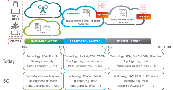
Figure 1: Transport network evolution towards 5G.
3. 5G transport network artchitecture and photonic systems
A relevant change is represented by the evolution of the radio access network and, specifically, by the transformation of the radio base station (RBS). Figure 2 shows the main steps of that transformation. A base station essentially consists of a baseband unit (BBU) and a radio unit (RU). The former includes all processing functions performed on the baseband signal, while the latter works on the radio frequency (RF) signal, and contains the antenna element, the RF power and low noise amplifiers, and the circuitry for digital-to-analog and analog-to-digital conversion of the downlink and uplink signals, respectively. In the traditional monolithic implementation, both BBU and RU are integrated in the same rack and connected via an RF cable. Subsequently, the RBS was split so that one BBU handles a certain number of remote RUs (RRUs), saving equipment cost. This transformation simplifies the deployment because the RRUs are simpler to install and configure, so reducing the operational expenditures, and allows a better coordination among RRUs connected to the same BBU. The typical distance between BBU and RRU is of the order of some hundred meters up to few kilometers.
To allow that transformation, it was necessary to introduce a new type of interface, named fronthaul, and related communication protocols. The most common one is named CPRI (common public radio interface) [6], based on a frame able to carry digitized IQ antenna samples while respecting tight requirements in terms of clock frequency accuracy, latency and synchronization of data in uplink and downlink. That interface can adapt to any radio standard but is bandwidth angry. For instance, to carry 40 MHz of radio bandwidth, corresponding to about 150 Mbit/s of true traffic, results to 2.5 Gbit/s CPRI data rate. For this reason, the new 5G radio will introduce new fronthaul interfaces, based on a different split of functions between BBU and RRUs.
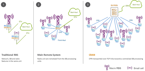
Figure 2: Radio access network evolution.
A second step of transformation was the introduction of the centralized RAN (C-RAN). In a C-RAN, the packet processing features asynchronous to the Hybrid Automatic-Repeat-Request (HARQ) loop, such as the Packet Data Convergence Protocol (PDCP) are centralized, as well as most of the Radio Control Functions (RCF), which are in charge of the load sharing among system areas and different radio technologies, the policies to control the schedulers in baseband and packet processing functions, the negotiation of QoS, etc. The centralization of those functions allows network operators to simplify their network architecture and management and to reduce the number of sites to lead to a further cost reduction especially in terms of operational expenditures. Packet processing and control functions can eventually be virtualized on generic purpose processors (GPPs), for example hosted in a data center, leading to the concept of cloud RAN. Even time critical baseband processing functions (BBFs) can be centralized but virtualization is more critical in this case so that they are more suitable for specific purpose processors (SPPs). Depending on the time sensitivity of the fronthaul interface between RRU and BBU, the maximum distance between RRU and BBU ranges from few kilometers up to few tens of kilometers.
All these transformations of the RBS and of the RAN lead to important changes in transport network. Probably, the most important one is that fronthaul, which was introduced as a point-to-point link between one BBU and one RRU, becomes a new transport segment with its peculiar requirements, distinguished by the backhaul segment responsible for the communication between the RBS and the rest of the network up to the mobile core network. Backhaul networks usually consist of aggregation nodes and links based on Ethernet transmission frames and packet switches (either Ethernet switches or MPLS/IP routers).
Fronthaul network instead, having to fulfill the tight requirements specified above, requires new architecture, nodes, and related photonic component and modules.
4. Photonics for data centers
Data centers (DCs) are the cornerstone of current social networks and are key elements of future 5G networks. They shall sustain the huge increase of network traffic while being increasingly green (i.e. consume less and less energy). The architecture of data centers is evolving in the last decade, passing from a hierarchical to a flat architecture [7], in which a huge number of servers must be connected to each other and to storage elements, besides being connected towards the outside world. Photonics is already playing a relevant role in DCs through a massive use of optical interconnections (basically point-to-point links). The evolution towards flat architectures will eliminate a huge number of OE/EO converting elements so that, besides photonic interconnect, photonic switching will emerge as a key technology [2,3,8,9]. If nowadays there is an internal packet aggregation interconnect network consisting of packet switches, in the future photonic switching could offload part of that work by introducing a given amount of circuit switching, for example to route long-lasting data flows that are most of internal data traffic volumes [4,10]. In this way the long lasting data flows are photonic switched while all the other are individually (packet-by-packet) switched in the electrical domain. The offloading of packet switches work also leads to improvement in the performance of short-lasting flows routing. The main benefit of the photonic switches is a dramatic reduction of both energy consumption and latency, while keeping the advantages of the CMOS scalable technology used for electrical packet switching in ensuring an ever-increasing processing capacity. Photonic switching can also provide an increased flexibility in the intra-DC interconnection among servers and storage elements to optimize the resources utilization. Nowadays there are static optical shuffles that are responsible for that function. Instead, a flexible and reconfigurable optical data center could provide a coordinated control of network resources and the capability to allocate dynamically the network capacity. This is made possible by re-applying the concept of SDN control and network function virtualization in the DC domain, in conjunction with a flexible photonic switched data plane.
Photonic switches suitable for those applications need to be highly integrated, low-cost, low-footprint, and high radix (64x64 or above). Silicon photonics is the most promising technology for that, and relevant examples are [11].
5. Photonic interconnect for future HW platforms
The always increasing traffic to be managed by telecom networks will require not only increasingly higher transmission capacity but also a huge increase of processing capabilities in different nodes like data centers, baseband processing units and so forth. This means that the corresponding hardware platforms will have to scale up accordingly. The Moore Law contributes to match these requirements indicating a path for the increase of the capacity of integrated electronic circuits (e.g. ASICs, network processors etc.); but it is not enough since the demand of processing capability grows faster than the miniaturization possibilities foreseen by the Moore Law. Thus, parallelization of ASICs is necessary, as well as the increase the data speed at the I/O ports. This means that if on one hand the processing capability of a single chip will increase, on the other hand there is a larger number of high speed interconnections allowing the interoperation of multiple ASICs on the same board (and among different boards). Since I/O pads and packages cannot scale enough, the transmission lines, able to interconnect each chip to each other, must work at higher bit rate. Unfortunately, the speed of the electric transmission lines in the board is going reach the upper bound, due to the frequency dependent loss that will soon become unacceptable. The only way to overcome this problem is to move towards photonic transmission lines on the board, whose losses are less dependent on bitrate and length. The use of such photonic onboard interconnect will allow to increase the bandwidth density (i.e. transmitted bit/s per mm2) of future harware platforms.
Practical photonics based solutions to achieve that are: the silicon interposer and the optical multi-chip module [12,13], and the starboard concept [13]. Figure 3 shows the Teraboard approach. The optical multi-chip module includes different integrated elements: a high capacity digital processor, a photonic array of transceivers, and an analog frontend to drive the photonic circuit and amplify the signals. In this way, the electrical interconnect is limited to very short transmission lines (1-2 cm max), while the photonic starboard accomplishes the photonic interconnect between different optical multi-chip modules. Such a starboard consists of a multi-layer glass block where many photonic waveguides are scribed and act as a photonic shuffle with extremely compact footprint and very low losses.
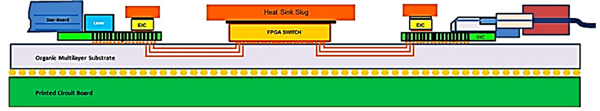
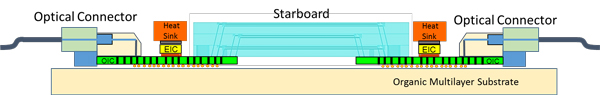
igure 3: TFop picture represents the optical multi-chip module. Bottom picture shows the starboard interconnecting two optical multi-chip modules.
6. Integrated photonics for 5G networks
As it has largely been experimented in tens of years in microelectronics, integration allows putting more and more functions and circuits on the same chip, leading to significantly lower assembly and test cost, besides a reduction of footprint and energy given by the miniaturization process. Of course the total cost of the component will come dependent on the yield of the fabrication process. In photonics, the basic technology for the devices is the InP, since lasers, photonic amplifiers and photodetectors are based on alloys III-V (e.g. InGaAsP heterostructures confined by InP). This because InP is a direct bandgap material able to easily generate and amplify light. Electronic elements can be realized as well with that technology. There are already commercial products based on InP photonic integrated circuits, like monolithically integrated multi-wavelength transceivers working up to 100Gbit/s [14]. However, the InP process technology never reached the performance of Silicon technology and thus the fabrication yield is low in comparison with CMOS technology. This limits the number of functions that can be integrated in a monolithic InP chip. Instead the well-developed Silicon process infrastructure, matured in many decades, allowed the implementation of very large scale integration system-on-chip and led to the development of highly integrated CMOS devices. If light generation and amplification cannot be achieved in Silicon, all the other photonic functions can be realized instead, such as modulators, detectors (Germanium monolithically integrated in Silicon), waveguides, de-multiplexers, power splitter etc. In addition, the high index contrast of Silicon enables the realization of more confined waveguides and miniaturized circuits (with respect to InP), and the tight integration with the electronics can be realized on the same chip area. Although the level of miniaturization cannot be of the same level as in the electronics, because the size of photonic elements and circuits is quite large in comparison to the size of a single transistor, it is still significant. For instance, in [15] was reported an integrated photonic system on chip accomplishing something like 1000 features in a few square millimeters device.
In summary, a complete photonic integrated circuit will need some InP based elements (i.e. lasers and semiconductor optical amplifiers) to be integrated with a Silicon chip through some kind of techniques, such as flip-chip [16], evanescent coupling [17] and template-assisted bonding [18].
Silicon photonics is the basic technology for many of the photonic components and modules mentioned in this paper: integrated transceivers, photonic switches for transport and for data centers, photonic interconnects for future HW platforms, as well as to accomplish some optical feature in radio sub-systems such as phase shifters, ultra-high frequency carrier generation.
Acknowledgements
The author wishes to thank Fabio Cavaliere, Paola Iovanna, and Francesco Testa for useful discussions.
References:
1.Ericsson, “5G Systems”, White Paper, January 2017.
2.T. A. Strasser, and J. L. Wagener, “Wavelength-Selective Switches for ROADM Applications”, IEEE Journal of Selected Topics in Quantum Electronics, vol. 16, Issue 5, Sept.-Oct. 2010.
3.V. Eramo, M. Listanti, R. Sabella, and F. Testa, “Definition and Performance Evaluation of a Low-Cost/High-Capacity Scalable Integrated OTN/WDM Switch”, IEEE Journal of Optical Communications and Networking, vol. 4, Issue 12, pp. 1033-1045 (2012)
4.R. Sabella, F. Testa, P. Iovanna, and G. Bottari, “Flexible packet-optical integration in the cloud age: Challenges and opportunities for network delayering”, IEEE Communications Magazine, vol. 52, Issue 1, Jan 2014
5.B. Skubic, J. Chen, J. Ahmed, L. Wosinska, B. Mukherjee, “A comparison of dynamic bandwidth allocation for EPON, GPON, and next-generation TDM PON”, IEEE Communications Magazine, Vol. 47, Issue 3, Mar 2009.
6.CPRI Specification V7.0 (2015-10-09) Interface Specification [Online]. Available: http://www.cpri.info/downloads/CPRI_v_7_0_2015-10-09.pdf.
7.W. Miao, F. Yan, N. Calabretta, “Towards Petabit/s All-Optical Flat Data Center Networks Based on WDM Optical Cross-Connect Switches with Flow Control”, IEEE Journal of Lightwave Technology, vol. 34, Issue 17, Sept.1, 2016
8.F. Testa, L. Pavesi, Optical Switching in Next Generation Data Centers, Springer International Publishing, 2018
9.A. Vahdat, H. Liu, X. Zhao, C. Johnson, “The emerging optical data center,” in Proceedings of OFC, 2011.
10.N. Farrington, G. Porter, S. Radhakrishnan, H.H. Bazzaz, V. Subramanya, Y. Fainman, G. Papen, A. Vahdat, ”Helios: a hybrid electrical/optical switch architecture for modular data centers.” in SIGCOMM’10, New Delhi, India, 30 August–3 September 2010
11.F. Testa, A. Bianchi, M. Romagnoli, “ Silicon Photonics Switch Matrices: Technologies and Architectures”, in Optical Switching in Next Generation Data Centers, Springer International Publishing 2018.
12.Ashok V. Krishnamoorthy et al., “From Chip to Cloud: Optical Interconnects in Engineered Systems,” IEEE Journal of Lightwave Technology, Vol.35,N. 15, Aug. 1, 2017.
13.H2020 Teraboard, European Project, http://www.teraboard.eu.
14.Fred Kish et al., “System-on-Chip Photonic Integrated Circuits,” IEEE Journal of Selected Areas in Quantum Electronics, VOL. 24, NO. 1, JANUARY/FEBRUARY 2018.
15.F. Testa et al., “Design and Implementation of an Integrated Reconfigurable Silicon Photonics Switch Matrix in IRIS Project,” IEEE Journal of Selected Areas in Quantum Electronics, VOL. 22, NO. 6, NOVEMBER/DECEMBER 2016.
16.R.A. Budd, L. Schares, B.G. Lee, F.E. Doany, C. Baks, D.M. Kuchta, C.L. Schow, F. Libsch, “Semiconductor optical amplifier (SOA) packaging for scalable and gain-integrated silicon photonic switching platforms,” in IEEE 65th Electronic Components & Technology Conference (ECTC), 2015.
17.H. Duprez, et al., “Heterogeneously Integrated III-V on Silicon Distributed Feedback Lasers at 1310 nm”, in Proceedings of OFC 2015, paper Tu3I.6.
18.Elton Marchena, Timothy Creazzo, Stephen B. Krasulick, Paul K. L. Yu, Derek Van Orden, John Y. Spann, Christopher C. Blivin, John M. Dallesasse, Petros Varangis, Robert J. Stone, and Amit Mizrahi, “ Integrated Tunable CMOS Laser for Si Photonics”, in Proceedings of OFC 2013, paper PDP5C.7.
 Roberto Sabella (M’78–SM’81–F’87) is the leader of Optical Systems unit of Ericsson Research, based in Pisa, Italy, and Montreal, Canada. His expertise covers several areas of telecom networks, such as packet-optical transport, optical solutions for mobile backhaul and fronthaul, and photonics technologies for radio and data centers. He has authored more than 150 papers published on international journals, magazines, and conferences, two books on optical communications, and holds more than 30 patents. He was adjunct professor of telecom systems at the Sapienza University of Rome. He is a senior member of IEEE and has guest edited many special issues in several IEEE journals and magazines. He holds the “laurea degree” in electronic engineering from the University of Rome “La Sapienza”, Italy
(FROM IEEE 5G ORG https://5g.ieee.org/)